A practical guide for engineering selection, service diagnostics, and assembly documentation. Correct pin identification and standardized sketches greatly reduce reverse-connection damage and batch mix-ups.
Most TO-can laser diodes (LD) look simple—only three pins. Inside the package, however, there is usually both a laser emitter (LD) and a monitor photodiode (PD) sharing a common terminal. The hardest field mistakes are therefore: which pin is which polarity, which pin is common, and whether the sketch viewing direction is mirrored.
This article reorganizes investigation methods, electrical checks, and sketch rules into one reusable workflow—especially useful when a full datasheet is missing and only SKU or marking information is available.
1. Understand the Structure First: LD, PD, and Common
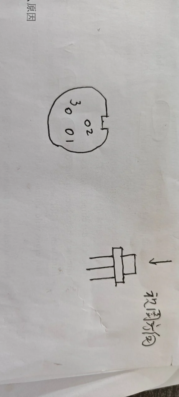
A typical visible / IR TO-can contains:
1. LD (emitter): the semiconductor laser chip that produces the beam. 2. PD (monitor): senses output power for APC (automatic power control). If closed-loop monitoring is not required, the PD may be left unused. 3. Common terminal: the shared electrode of LD and PD; in many packages it is tied to the metal case.
Three pins do not mean “anode / cathode / transistor control.” Treating the third pin as a “transistor gate” is a common misconception. For laser diodes, the third pin is normally related to the PD or common network and must be confirmed by datasheet or measurement.
2. Common Internal Configurations: N, P, and M Types
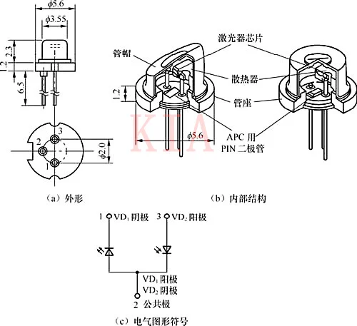
By common-terminal polarity, field practice often groups packages as:
| Type | Common meaning | Key point |
|---|---|---|
| **N-type** | Common cathode | Common is on the cathode side; LD/PD anodes are brought out separately |
| **P-type** | Common anode | Common is on the anode side |
| **M-type** | Mixed / series-like | LD and PD polarities are interleaved; always check the schematic |
Pin numbers (1/2/3) and notch positions are not universally standardized across vendors. Even when “pin 2 sits at the notch,” the internal network may still be common-anode or common-cathode. Pin numbers only fix geometry; polarity must be labeled separately.
3. Four Practical Identification Methods
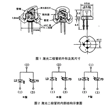
3.1 Model / Datasheet Investigation (preferred)
1. Look up the product model from the SKU in your ERP / shop system (e.g. ShopElf). 2. Retrieve the datasheet and check Pin Assignment / Outline. 3. If the model is unknown, use case marking / lot code to trace the OEM part number, then match the datasheet.
When a datasheet exists, do not guess pins by intuition.
3.2 Multimeter Diode Mode (red / IR)
Useful for red and infrared LDs with operating voltage around ~2 V:
– LD forward drop: about ~2 V – PD forward drop: about ~0.8 V – LD+PD combined signature: often around ~2.8 V (depends on probe polarity combinations)
Tip: probe pin pairs in diode mode, separate LD vs PD branches by voltage magnitude, then map polarity against the case/common relationship.
Note: green and higher-threshold diodes may show almost no reading in diode mode—do not force a conclusion with this method alone.
3.3 Threshold-Voltage Trial Contact (green, etc.)
When datasheet is missing and diode-mode fails:
1. Use a regulated supply near the diode threshold / start-up voltage. 2. Under current limiting, briefly trial-contact pin combinations. 3. Watch for emission to identify LD polarity.
Always limit current, keep contacts short, and avoid overshoot. Hard-applying voltage without limiting can destroy the LD instantly via surge current.
3.4 Resistance Method to Separate LD / PD (supplementary)
With a resistance range (e.g. R×1k), rough checks are possible (highly meter- and aging-dependent):
1. Separate LD vs PD: among the three pin pairs, one reading often falls in the kilo-ohm range and helps identify the PD side vs common; the remaining pin is then associated with the LD side. 2. Check PD: forward of a few kΩ and reverse open usually looks healthy; 0 / open forward, or leaky reverse, suggests a bad PD. 3. Check LD: forward often roughly 10–30 kΩ with reverse open; very high forward plus reduced reverse may indicate severe aging.
Resistance checks do not replace a datasheet and do not authorize high-current operation.
4. How to Draw Pinout Sketches Without Mirroring Errors
The recommended field record is a hand-drawn top-view sketch with notch, plus an explicit viewing-direction note.
Recommended sketch rules
1. Draw a circle with a flat / square notch for package orientation. 2. Mark three pin dots and number them 1, 2, 3. 3. Numbering is commonly counter-clockwise, with pin 2 at the notch (state your convention beside the sketch). 4. Lock the viewing direction: prefer a top view looking from the emission aperture (cap window) down toward the pins, not looking upward from the lead side (which mirrors left/right). 5. After geometry matches the physical part, annotate polarity text for pins 1/2/3, for example: – 2 = LD+ / PD− (common) – 1 = LD− – 3 = PD+ (Example wording only—always follow the actual part.)
Batch-card checklist
– Model / SKU / marking – Viewing direction (top view from aperture) – Relative positions of 1/2/3 vs notch – Polarity labels: LD+, LD−, PD+, PD−, Case – Internal type: N / P / M (if known) – Test method and results – Date and recorder
A clear sketch usually prevents more reverse-wiring errors than verbal handoff alone.
5. Handling and Safety Notes
1. Never hard-apply voltage without current limiting; surge/overshoot can destroy the LD. 2. ESD protection: use a grounded wrist strap (often with 1 MΩ series resistance). 3. Soldering: ground the iron shell or unplug it; keep about 260 °C and short time (e.g. < 5 s). 4. Operating current: do not exceed ratings during tuning; avoid uncontrolled current if a lead opens mid-adjust. 5. Eye safety: never view the beam directly or via specular reflection; apply laser warning labels as required.
6. Recommended Workflow
1. Identify the model first: SKU → part number → datasheet pinout. 2. Measure only if needed: diode mode for red/IR; threshold trial for green. 3. Sketch immediately: top view + notch + 1/2/3 + polarity text. 4. Recheck before assembly: compare sketch vs physical notch; reject mirrored drawings. 5. Archive: keep sketch photos with lot records.
Closing
Laser diode pinout work is really two tasks: record geometry (which pin) separately from electrical meaning (what polarity), then use one consistent top-view sketch rule so viewing direction never flips the map.
Once investigation, measurement, and sketch standards become team habit, selection, repair, and batch assembly become faster—and far fewer diodes fail on first power-up.
*Editorial note: rewritten from source materials titled “激光二极管脚位辨析和草图记录的方法,” with incorrect transistor-pin descriptions removed and the content restructured as a knowledge article.*